Circuitry was designed in 130nm CMOS technology which achieved low power operation of 19mW with modern supply voltage of 12v and fast 01 settling time of less than 49ns for load capacitance of 5pF with output swing of 1v to 11v and input Common Mode Range of 05v with large CMRR and PSRR of more than 124dB and 74dB respectively due to. Lecture 23 Design of Two-Stage Op Amps 31116 Page 23-10 CMOS Analog Circuit Design PE.
Cadence Tutorial Operational Amplifier Design In Cadence Part 1b Diff Amp Design Youtube
Design for S 5 from the minimum input voltage.
. Coding and simulation is done in T-Spice and. Operational Transconductance Amplifier OTA Compensator Design Operational. CL input enter the value of slew rate CL.
Introduction to CMOS Analog VLSI Design contd. A classic wanting design that caters to diamonds squares and circles. Introduction to CMOS Analog VLSI Design.
A comparison has been made between scaled voltage supply and power consumption. VDS5sat Vinmin -VSS-I5 1. Vos Vos1 2 Vos2 A1 2 When we refer the offset of the second stage at the input terminal we have to divide it by the gain of the first stage.
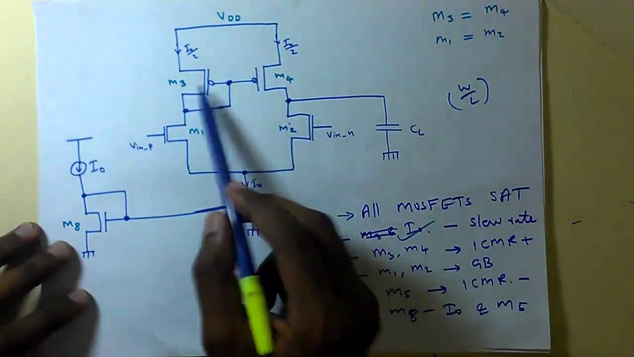
Basic of MOS Amplifier part-1 6Lecture 6. 3a shows a basic differen- tial input OTA with one current-mirror. G m1 GB.
1Lecture 1. Cmos ota design tutorial. C c S 2 g m1 2 K 1 I 5 6.
12 International Journal of Managing Public Sector Information and Communication Technologies IJMPICT Vol. Io gmIabcV 1-V2 VCVS The transconductance gain gm is a function of the gm h1 Iabc for bipolar and weak inversion MOSFETs gm h2 Iabc 12. Next we discuss the basic transconductor OTA topolo- gies with differential inputs.
Read Online Design Of Operational Transconductance Amplifier Analysis Of Schematic Circuit And Cmos Layout Of Ota tsunamiasgov Glossary - All Terms and Definitions Listed Alphabetically TUTORIAL CADENCE DESIGN ENVIRONMENT - AnasayfaN. First calculate V DS5 sat then find S 5. The operation of cmos inverter can be studied by using simple switch model of mos transistor.
Section 4 presents our two-stage OTA design and the simulation results. Basic of MOS Amplifier Part-3. Layout has done using Microwind 2 and schematic is designed using DSCH software.
The CMOS OTA is designed in 255nm CMOS technology with 10V power supply to observe the configurations. Determine g m from design objectives dynamic range bandwidth 2. Section 2 includes a discussion of circuit topology considerations for low power.
Analog Design for CMOS VLSI Systems Franco Maloberti The random offset is due to the geometrical mismatching and process dependent inaccuracies. Pick g m I D or f t Large g m I D low power large signal swing Small g m I D high f t high speed 4. Pennisi Design Procedure for Two-Stage CMOS Transconductance Operational Amplifiers.
It vid q - vl. The common-mode feedback 18 is not shown. 3b a balanced OTA with three current mirrors and a single out- put is shown.
Maloberti - Layout of Analog CMOS IC 32 Stick Layout. Fingers of M6 and M7 all together M6 90 M760 M1 and M2 in a common centroid arrangement. KN 30 µAV2 KP 10 µAV2.
2 June 2014 I5 SRCL Pdiss input. 1 and 2 the funda- 6. SR input enter the value of slew rate SR.
The operational transconductance amplifier has 1 V power supply and 113 µA input bias current. Pick L Short channel high f t high speed Long channel high intrinsic gain good matching. Should youre into unique and edgy nail artwork designs then That is something which you unquestionably should really try out.
AMPLIFIER OTA First commercial OTA produced by RCA in 1969 ie CA3080 Io V2 V1 Iabc. In design of CMOS OTA TANNER EDA TOOL is used. Design of CMOS OTA 25 MATLAB Code for extraction of designing parameter Vdd input enter the value of Vdd.
Exercise Draw the stick diagram of the two stages OTA in the following three cases. 1 has been designed by using a standard 12-µm CMOS technology which has the main following process parameters. Simulations In order to evaluate the accuracy of proposed proce-dure the two-stage OTA in Fig.
This ultimately results in increased bandwidth of OTA as can be seen from Table 1. The approach exploits the bulk terminal to set the output quiescent current of a two-stage class-AB CMOS OTA in a reliable manner and without reducing the maximum swing capability. 3c illustrates a fully differential OTA.
Abstract In this paper designing of MOS Transistors in two stages OTA has been done and simulated in 120nm technology. This tutorial provides a complete survey of CMOS multipliers presents a unified generation of multiplier architectures and proposes the most recommended MOS multiplier structure. Along with them is this design of operational transconductance amplifier analysis of schematic circuit and cmos layout of ota that can be your partner.
Cmos layout of ota and numerous books collections from fictions to scientific research in any way. Lengths of CMOS devices are scaled down both their channel delays and capacitive parasitic are reduced which increases the cut off frequencies of the transistors. Design for S 1 S 2 to achieve the desired GB.
Subscribe to electronics-Tutorial email list and get Cheat Sheets latest updates tips tricks about electronics- to your inbox. Section 3 outlines the approach we took to meeting the required specifications at a minimum power level. Basic of MOS Amplifier Part-2 7Lecture 7.
Che Ismail3 Design and Analysis of a Two-Stage OTA for Sensor Interface Circuit 2014 IEEE Symposium on Computer Applications Industrial Electronics ISCAIE April 7 - 8 2014 Penang Malaysia. Determine I D from g m and g m I D 5. OTA specifications The rest of this paper proceeds as follows.
The design flow which relates the performance to the design parameters is summarized in Table 1. This tutorial could serve as a starting reference point and metric for comparison of new CMOS multiplier circuit configurations. MOSFET-Amplifiers Analog-CMOS-Design- Electronics Tutorial.
Allen - 2016 Unbuffered Op Amp Design Procedure - Continued 5. -based Design Flow 1. Since the two offsets are uncorrelated we have.
Design simulation and testing of a two-stage CMOS operational transconductance amplifier by 018 µm complementary metal oxide semiconductor CMOS technology are described in this paper. Mental output component at each output is given by - q d A suitable architecture for low voltage power supply is while the differential output iod io - io2is -2a1vLdwhere the pseudo-dlfferential transconductance 19 20 221.
Schematic Of A Simple Cmos Stages Ota Download Scientific Diagram

Design Procedure For Two Stage Cmos Transconductance Operational Amplifiers A Tutorial Semantic Scholar

Electronics Free Full Text On The Sizing Of Cmos Operational Amplifiers By Applying Many Objective Optimization Algorithms Html

Pdf Comparative Analysis Of Cmos Ota Semantic Scholar

Fractal Fract Free Full Text Cmos Ota Based Filters For Designing Fractional Order Chaotic Oscillators Html

Activity 2 Stage Cmos Ota Analog Devices Wiki

Circuit Simulation Results Of An Ota In 250nm Cmos Process Afriditech

Opamp Circuit Design Tutorial Youtube
0 comments
Post a Comment